Merging CPUs and GPUs
AMD has already outlined the beginning of its CPU/GPU merger strategy in a little product called Fusion. While quite bullish on Fusion, AMD hasn't done a tremendous job of truly explaining the importance of Fusion. Fusion, if you haven't heard, is AMD's first single chip CPU/GPU solution due out sometime in the 2008 - 2009 timeframe. Widely expected to be two individual die on a single package, the first incarnation of Fusion will simply be a more power efficient version of a platform with integrated graphics. Integrated graphics is nothing to get excited about, but it is what follows as manufacturing technology and processor architectures evolve that is really interesting.
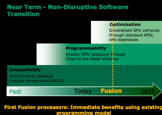
AMD views the Fusion progression as three discrete steps:
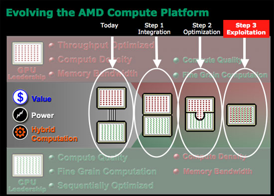
Today we have a CPU and a GPU separated by an external bus, with the two being quite independent. The CPU does what it does best, and the GPU helps out wherever it can. Step 1, is what AMD is calling integration, and it is what we can expect in the first Fusion product due out in 2008 - 2009. The CPU and GPU are simply placed next to one another and there's minor leverage of that relationship, mostly from a cost and power efficiency standpoint.
Step 2, which AMD calls optimization, gets a bit more interesting. Parts of the CPU can be shared by the GPU and vice versa. There's not a deep level of integration, but it begins the transition to the most important step - exploitation.
The final step in the evolution of Fusion is where the CPU and GPU are truly integrated, and the GPU is accessed by user mode instructions just like the CPU. You can expect to talk to the GPU via extensions to the x86 ISA, and the GPU will have its own register file (much like FP and integer units each have their own register files). Elements of the architecture will be shared, especially things like the cache hierarchy, which will prove useful when running applications that require both CPU and GPU power.
The GPU could easily be integrated onto a single die as a separate core behind a shared L3 cache. For example, if you look at the current Barcelona architecture you have four homogenous cores behind a shared L3 cache and memory controller; simply swap one of those cores with a GPU core and you've got an idea of what one of these chips could look like. Instructions that can only be processed by the specialized core will be dispatched directly to it, while instructions better suited for other cores will be sent to them. There would have to be a bit of front end logic to manage all of this, but it's easily done.
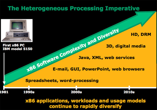
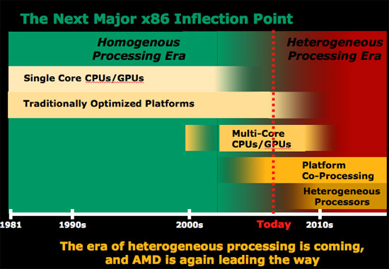
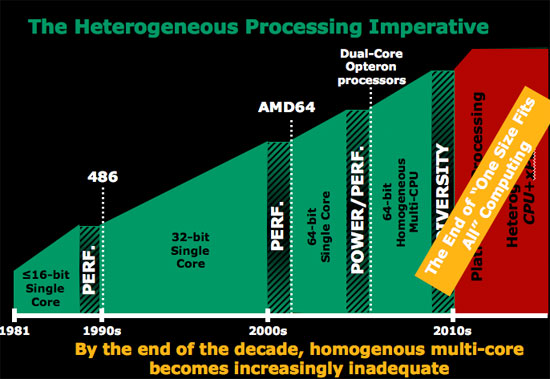
AMD went as far as to say that the next stage in the development of x86 is the heterogeneous processing era. AMD's Phil Hester stated plainly that by the end of the decade, homogeneous multi-core becomes increasingly inadequate. The groundwork for the heterogeneous processing era (multiple cores on chip each with a different purpose) will be laid in the next 2 - 4 years, with true heterogeneous computing coming after 2010.
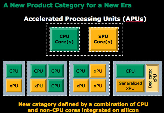
It's not just about combining the CPU and GPU as we know them; it's also about adding other types of processors and specialized hardware. You may remember that Intel made some similar statements a few IDFs ago, but not nearly as boldly as AMD given that Intel doesn't have nearly as strong of a graphics core to begin integrating. The xPUs listed in the diagram above could easily be things like H.264 encode/decode engines, network accelerators, virus scan accelerators, or any other type of accelerator that's deemed necessary for the target market.
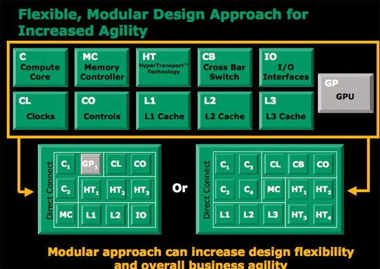
In a sense, AMD's approach is much like that of the Cell processor, the difference being that with AMD's direction the end result would be a much more powerful sequential core combined with a true graphics core. Cell was very much ahead of its time, and by the time AMD and Intel can bring similar solutions to the market the entire industry will be far more ready for them than it was for Cell. Not to mention that treating everything as extensions to the x86 ISA makes programming far easier than with Cell.
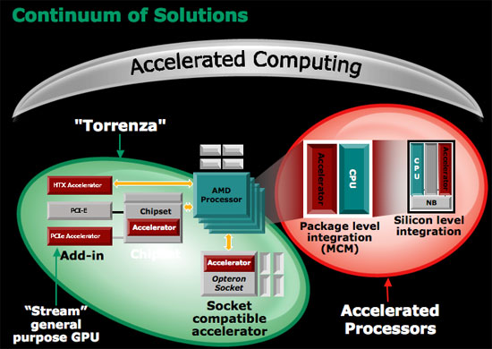
Where does AMD's Torrenza fall into play? If you'll remember, Torrenza is AMD's platform approach to dealing with different types of processors in an AMD system. The idea being that external accelerators could simply pop into an AMD processor socket and communicate with the rest of the system over Hyper Transport. Torrenza actually works quite well with AMD's Fusion strategy, because it allows for other accelerators (xPUs if you will) to be put in AMD systems without having to integrate the functionality on AMD's processor die. If there's enough demand in the market, AMD can eventually integrate the functionality on die, but until then Torrenza offers a low cost in-between solution.
AMD drew the parallel to the 287/387 floating point coprocessor socket that was present on 286/386 motherboards. Only around 2 - 3% of 286 owners bought a 287 FPU, while around 10 - 20% of 386 owners bought a 387 FPU; when the 486 was designed it simply made sense to integrate the functionality of the FPU into all models because the demand from users and developers was there. Torrenza would allow the same sort of migration to occur from external socket to eventual die integration if it makes sense, for any sort of processor.
AMD has already outlined the beginning of its CPU/GPU merger strategy in a little product called Fusion. While quite bullish on Fusion, AMD hasn't done a tremendous job of truly explaining the importance of Fusion. Fusion, if you haven't heard, is AMD's first single chip CPU/GPU solution due out sometime in the 2008 - 2009 timeframe. Widely expected to be two individual die on a single package, the first incarnation of Fusion will simply be a more power efficient version of a platform with integrated graphics. Integrated graphics is nothing to get excited about, but it is what follows as manufacturing technology and processor architectures evolve that is really interesting.

AMD views the Fusion progression as three discrete steps:

Today we have a CPU and a GPU separated by an external bus, with the two being quite independent. The CPU does what it does best, and the GPU helps out wherever it can. Step 1, is what AMD is calling integration, and it is what we can expect in the first Fusion product due out in 2008 - 2009. The CPU and GPU are simply placed next to one another and there's minor leverage of that relationship, mostly from a cost and power efficiency standpoint.
Step 2, which AMD calls optimization, gets a bit more interesting. Parts of the CPU can be shared by the GPU and vice versa. There's not a deep level of integration, but it begins the transition to the most important step - exploitation.
The final step in the evolution of Fusion is where the CPU and GPU are truly integrated, and the GPU is accessed by user mode instructions just like the CPU. You can expect to talk to the GPU via extensions to the x86 ISA, and the GPU will have its own register file (much like FP and integer units each have their own register files). Elements of the architecture will be shared, especially things like the cache hierarchy, which will prove useful when running applications that require both CPU and GPU power.
The GPU could easily be integrated onto a single die as a separate core behind a shared L3 cache. For example, if you look at the current Barcelona architecture you have four homogenous cores behind a shared L3 cache and memory controller; simply swap one of those cores with a GPU core and you've got an idea of what one of these chips could look like. Instructions that can only be processed by the specialized core will be dispatched directly to it, while instructions better suited for other cores will be sent to them. There would have to be a bit of front end logic to manage all of this, but it's easily done.


AMD went as far as to say that the next stage in the development of x86 is the heterogeneous processing era. AMD's Phil Hester stated plainly that by the end of the decade, homogeneous multi-core becomes increasingly inadequate. The groundwork for the heterogeneous processing era (multiple cores on chip each with a different purpose) will be laid in the next 2 - 4 years, with true heterogeneous computing coming after 2010.

It's not just about combining the CPU and GPU as we know them; it's also about adding other types of processors and specialized hardware. You may remember that Intel made some similar statements a few IDFs ago, but not nearly as boldly as AMD given that Intel doesn't have nearly as strong of a graphics core to begin integrating. The xPUs listed in the diagram above could easily be things like H.264 encode/decode engines, network accelerators, virus scan accelerators, or any other type of accelerator that's deemed necessary for the target market.

In a sense, AMD's approach is much like that of the Cell processor, the difference being that with AMD's direction the end result would be a much more powerful sequential core combined with a true graphics core. Cell was very much ahead of its time, and by the time AMD and Intel can bring similar solutions to the market the entire industry will be far more ready for them than it was for Cell. Not to mention that treating everything as extensions to the x86 ISA makes programming far easier than with Cell.

Where does AMD's Torrenza fall into play? If you'll remember, Torrenza is AMD's platform approach to dealing with different types of processors in an AMD system. The idea being that external accelerators could simply pop into an AMD processor socket and communicate with the rest of the system over Hyper Transport. Torrenza actually works quite well with AMD's Fusion strategy, because it allows for other accelerators (xPUs if you will) to be put in AMD systems without having to integrate the functionality on AMD's processor die. If there's enough demand in the market, AMD can eventually integrate the functionality on die, but until then Torrenza offers a low cost in-between solution.
AMD drew the parallel to the 287/387 floating point coprocessor socket that was present on 286/386 motherboards. Only around 2 - 3% of 286 owners bought a 287 FPU, while around 10 - 20% of 386 owners bought a 387 FPU; when the 486 was designed it simply made sense to integrate the functionality of the FPU into all models because the demand from users and developers was there. Torrenza would allow the same sort of migration to occur from external socket to eventual die integration if it makes sense, for any sort of processor.


55 Comments
View All Comments
tygrus - Saturday, May 12, 2007 - link
See latest low-power Athlon64 <10w idle. Can further reduce max power consumption (from 30-60w) if you limit the clock speed to about 1GHz and drop the voltage (<15w).TA152H - Sunday, May 13, 2007 - link
Tygrus,Idle isn't so important to me, getting to less than 1 watt idle isn't particularly hard if you go into sleep mode. You can't build a fanless, noiseless system based on idle performance. I was looking at Intel's ULV stuff too, but it's just not there either. It's kind of disappointing, because most people would be perfectly happy with a 1 GHz K6-III using 8 watts or less as it would on modern processes, and nothing like it is available. VIA's stuff sucks and I don't think is very efficient, even though they are targetting this market. My main machine I just upgraded to a Coppermine 600 on a weird Intel VC820 board. It's perfectly capable of doing just about everything I do, except for compiles (even a Core 2 is too slow for that, Microsoft seriously needs to work on parallelizing their compilers, or if they have recently, I need to buy it :P).
It's an enormous waste of electricity to sell these processors when the vast majority of people don't need them. To Microsoft's credit, they are always up to the challenge of releasing bloated software that requires more memory and processing power but is functionally the same, but at some point even their talent for this might run out.
While I was writing the first reply, I was lamenting about how lousy the current processors are in this respect, but then I read that at least AMD had a clue and said the Athlon design could not address this space and they had to go with something different. Maybe they'll bring the K6-III back, fix it's decoding/memory problems, and have a real winner. In terms of power/performance, there is just no beating it, these superpipelined processors are inherently poor at power use, and clearly have a performance bias. Why VIA went this way is a big mystery to me.
chucky2 - Friday, May 11, 2007 - link
If this article has accomplished one thing, it would be that we finally have confirmation that AM2+ CPU's will work in AM2 motherboards. Up to this point it's been people reporting on "sources" and stuff like that, nothing direct from AMD.Anand's report is more than good enough for me, I can finally rest easy that the PC I just built my cousin will have an upgrade path for at least another year down the road (if not two).
Thanks Anand and AMD! (and screw you Intel for you rediculously short upgrade paths!)
Chuck
AdamK47 - Friday, May 11, 2007 - link
Well played, Anand. Well played.Kiijibari - Friday, May 11, 2007 - link
I would have looked at my watch, while cinebench was running on the 4x4 system to get a rough estimate :)Not a correct result, but better than nothing.
Or was the system so fast, that cinebench was done after a few ns ^^ ? :)
Apart from that, nice article, thanks :)
cheers
Kiijibari
Anand Lal Shimpi - Friday, May 11, 2007 - link
I counted seconds in my head, out of fairness to AMD I didn't report the number I calculated :)Take care,
Anand
Sunrise089 - Friday, May 11, 2007 - link
Didn't you guys notice the huge disconnect between the excitement evident in Anand's text and the fairly small ammount of new info? I think it should be obvious that AMD revlealed a lot more, but they have put various NDA dates on when the info can be released. So I would say they did open up a lot, but that we will only see the new info become available as we get closer to Barcelona.Anand Lal Shimpi - Friday, May 11, 2007 - link
I think you have to shift your expectations a bit; going into this thing I wanted to see Barcelona performance, I wanted the equivalent of what Intel did with Penryn and Nehalem. I didn't get that, but what I did get was a much clearer understanding of AMD's direction for the future. The section on Fusion is of particular importance to the future of the company, it just so happens that AMD's strategy is in line with Intel's, lending credibility to what it is doing.Then there were a handful of Barcelona tidbits that I needed to stick in some sort of an article, so this one just seemed the best venue to do so. More information is coming though, stay tuned for next week. No benchmarks yet unfortunately :(
Take care,
Anand
Stablecannon - Friday, May 11, 2007 - link
Wonderful. So basically this article was an AMD morale booster.
"Hey this Phil Hester, just wanted to say don't lose faith in us, even though we don;t have anything to show you really...that's because it's a secret. Yeah, that's it. We actually have a 16 core chip running at 3.8 that'll cream Intel. What's that? You want to see it? LOL."
TA152H - Friday, May 11, 2007 - link
First of all, I read the part about AMD becoming much more forthcoming with information, and then saw essentially nothing new in the article. Pretty much all of this stuff is known, and the important stuff you still don't know. So, how are they so much more open again? I didn't see it.Actually, I would have been disappointed if they were. I mean, you can scream about how they're not giving you what YOU want, but it's all about what they want. I don't buy them giving information out too early for Intel, you can be pretty sure there are plenty of companies designing products around AMD's new chip and you can be pretty sure at least one person has "slipped" and told Intel something. It's more likely it's not to AMD's benefit to have people knowing it's so much better than what's out now. How do they move product they are making today when people are waiting for their next great product? It's just common sense, they don't care if people whine about lack of visibility, too much is worse than too little. They have given out some numbers, and they are very high, so I doubt they're too concerned about performance. I think they're more concerned about selling stuff they have out today, which they aren't doing a great job of. What would happen if they showed a great product right around the corner? Q1 would look like a success compared to what they'd endure.
When you talk about Phil Hester you have to realize this guy referred the 8088 an eight-bit architecture (so he was not referring to the data bus). After that, I don't know what to think about what he says.
Next, the reason the 287 didn't sell was because it seriously sucked! It was worse than the 8087 because it didn't even run synchronously with the processor. Considering the 286 was way more powerful than the 8086/8088, there was a perfectly good reason why no one wanted a math coprocessor that was expensive, generally ran at 2/3 CPU speed (unless a seperate crystal was put in for it, which was done with later 286 machines), and actually had less performance than the 8087. The 387 was much more powerful and totally redesigned.
Also keep in mind the 486 was later made in an incarnation called the 486SX, that had either a disabled or no math coprocessor on it.
Saying the Cell is before it's time is implying it's fundamentally a useful product, but other things around it have to catch up. That's wrong and misleading. It's a niche product and it's a bear to program and is terrible in most things besides what it was designed for. Time won't change it, unless they change the Cell. The way it is now, it'll never be anything more than a niche product, nor was it designed to be more than that.
For their < 1 watt processors, it might be interesting to see if they bother with a decoupled architecture. My guess is they'll just run x86 instructions natively, without wasting so much silicon on the decoders.
With regards to AMD's next processor taking so long, I think it's even worse when one considers the K8 isn't really a K8 at all, it's more like a K7+. It's very similar to the K7, and is far less of a jump than the Prescott was from the Northwood. It's more like the Pentium MMX was to the Pentium (I'm not talking about the MMX instructions, there was a lot more changes than that).
The remarks about AMD coming back from this stronger than ever are absurd and ridiculous. They can come back, and they certainly have a good product in the wings, but it's got nothing to do with losing $611 million. It weakened the company, plain and simple, although not irrevocably. They had to slow down their investment and conversion, which isn't good. They had to sell $2 Billion in debts at very disadvantageous terms. Both of these are injuries that will have longer term ramifications for the company. So, yes, they aren't dead, but saying this will make them stronger in the long run is plain wrong and equally weird.