ASUS P5E3 Premium: Features and BIOS Changes
The P5E3 Premium board is designed for the general enthusiast with an emphasis on features designed for the home user, whether it is for gaming or home theater usage. ASUS provides two eSATA ports via the JMicron JMB363 chipset, IEEE 1394 support from Agere, excellent on-board audio support from the ADI 1988B, an 802.11n Wireless port, and dual Gigabit LAN capability.
The board offers a very good mix of expansion slots although utilizing a CrossFire setup will create the physical loss of a PCI Express x1 and PCI slot. The third PCI Express x16 slot operates at x4 electrically and can be utilized for various PCI Express cards including AGEIA PhysX, RAID controllers, or a third video card at this time.
We will go into the BIOS settings in additional detail once we receive the retail kit and official launch BIOS. However, the following screenshots represent features that we know will be in the retail BIOS.
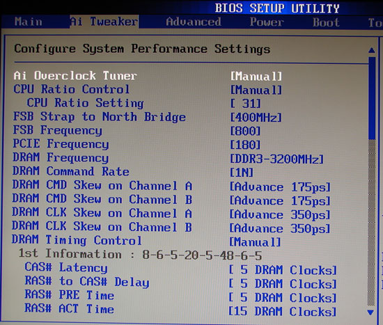
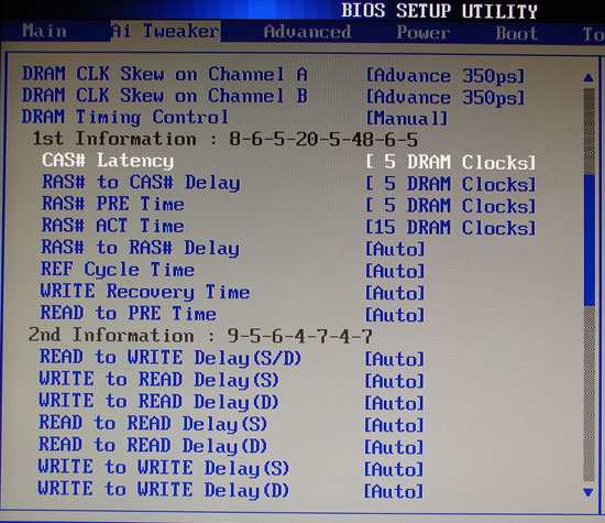
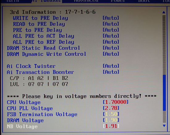
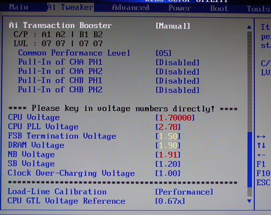
The P5E3 Premium BIOS has undergone a makeover of sorts. The AI Tweaker section is still in place with a wide variety of options for tuning the board. Although not as extensive as the latest DFI enthusiast boards, the options available have been expanded. The notable addition being the revamped the Transaction Booster setting. The Transaction Booster option is actually another name for tRD (Performance Level) and can be adjusted from 31 down to 1. ASUS joins DFI now in offering this setting that greatly affects latencies and overall system performance. The DRAM timing control sections now offers 23 different memory settings.
Our screenshots show the maximum value for each option. ASUS has listened to the power users and now offers CPU voltages to 2.10V and MCH voltages to 2.21V provided the OC jumper on the motherboard is enabled. ASUS has also included the ability to save BIOS profiles, although it is currently limited to two profiles.
| ASUS P5E3 Premium | |
| Market Segment | High Performance Enthusiast - $299.99 (estimated) |
| CPU Interface | Socket T (Socket 775) |
| CPU Support | LGA775-based Core 2 Duo, Core 2 Extreme, or Core 2 Quad Recommended |
| Chipset | Intel X48 (MCH) Northbridge and ICH9R Southbridge |
| FSB Speeds | Auto, 200 ~ 800 in 1MHz increments |
| Memory Speed (DDR3) | Auto, Eight Ratios dependent upon Strap Setting |
| FSB Strap | Auto, 200, 266, 333, 400 |
| PCIe Speeds | Auto, 100MHz - 180MHz |
| PCI Speeds | Locked at 33.33MHz |
| Core Voltage | Auto, 1.10000 to 1.70000 in .00625 increments, plus settings to 2.10V with OC jumper enabled. |
| CPU Clock Multiplier | 6x ~ 12x, downward adjustable for Core 2, upward to 31 for Extreme |
| DRAM Voltage (DDR3) | Auto, 1.50V ~ 2.78V in .02V increments, 1.50V standard |
| DRAM Timing Control | Auto, Manual - 23 DRAM Timing Options (tCL, tRCD, tRP, tRAS, tRFC + 18 sub-timings) |
| DRAM Command Rate | Auto, 1N, 2N |
| NB Voltage | Auto, 1.25V ~ 1.91V in .02V increments, plus settings to 2.21V with OC jumper enabled. |
| SB Voltage | Auto, 1.05V, 1.20V, 1.05V standard |
| FSB Termination Voltage | Auto, 1.20V to 1.50V in .02V increments, 1.20V standard |
| Clock Over Charging | Auto, .70V to 1.00V in .10V increments, .80V standard |
| CPU Voltage Damper | Auto, Enabled, Disabled |
| CPU Voltage Reference | Auto, .67, .65, .63, .62 |
| NB Voltage Reference | Auto, .67, .61 |
| AI Clock Twister | Auto, Light, Medium, Strong |
| DRAM CLK Skew CA/CB | Auto, Normal, 50ps to 350ps either advance or decrease |
| DRAM CMD Skew CA/CB | Auto, Normal, 25ps to 175ps either advance or decrease |
| AI Transaction Booster (tRD) | Auto, Manual, settings from 31 to 1 |
| Memory Slots | Four 240-pin DDR3 DIMM Slots Dual-Channel Configuration Regular Unbuffered DDR3 Memory to 8GB Total |
| Expansion Slots | 3 - PCIe x16 (2 - x16, 1 - x4 electrical) 2 - PCIe x1 2 - PCI Slot 2.2 |
| Onboard SATA/RAID | 6 SATA 3Gbps Ports - ICH9R (RAID 0,1, 10, 5) 2 eSATA 3Gbps Port - JMicron JMB363 |
| Onboard IDE | 1 ATA133/100/66 Port (2 drives) - JMicron JMB363 |
| Onboard USB 2.0/IEEE-1394 | 10 USB 2.0 Ports - 6 I/O Panel - 4 via Headers 2 FireWire 400 Ports by Agere FW3227 - 1 I/O Panel, 1 via Header |
| Onboard LAN | Realtek RTL8110SC - PCI Gigabit Ethernet controller Marvell 88E8056 PCI Express Gigabit Ethernet controller ASUS 802.11n Wireless Port |
| Onboard Audio | ADI 1988B - 8-channel HD audio codec |
| Power Connectors | ATX 24-pin, 8-pin ATX 12V |
| I/O Panel | 1 x PS/2 Keyboard 2 x eSATA 2 x SPDIF - Optical Out, Coaxial Out 1 x IEEE 1394 1 x Audio Panel 2 x RJ45 6 x USB 2.0/1.1 |
| Fan Headers | 6 - CPU, (5) Chassis |
| Fan Control | CPU and Chassis Fan Control via BIOS/AI Suite, PC Probe II monitoring |
| BIOS Revision | v110 |
| Board Revision | v1.00 |
The P5E3 Premium board is designed for the general enthusiast with an emphasis on features designed for the home user, whether it is for gaming or home theater usage. ASUS provides two eSATA ports via the JMicron JMB363 chipset, IEEE 1394 support from Agere, excellent on-board audio support from the ADI 1988B, an 802.11n Wireless port, and dual Gigabit LAN capability.
The board offers a very good mix of expansion slots although utilizing a CrossFire setup will create the physical loss of a PCI Express x1 and PCI slot. The third PCI Express x16 slot operates at x4 electrically and can be utilized for various PCI Express cards including AGEIA PhysX, RAID controllers, or a third video card at this time.
We will go into the BIOS settings in additional detail once we receive the retail kit and official launch BIOS. However, the following screenshots represent features that we know will be in the retail BIOS.


The P5E3 Premium BIOS has undergone a makeover of sorts. The AI Tweaker section is still in place with a wide variety of options for tuning the board. Although not as extensive as the latest DFI enthusiast boards, the options available have been expanded. The notable addition being the revamped the Transaction Booster setting. The Transaction Booster option is actually another name for tRD (Performance Level) and can be adjusted from 31 down to 1. ASUS joins DFI now in offering this setting that greatly affects latencies and overall system performance. The DRAM timing control sections now offers 23 different memory settings.
Our screenshots show the maximum value for each option. ASUS has listened to the power users and now offers CPU voltages to 2.10V and MCH voltages to 2.21V provided the OC jumper on the motherboard is enabled. ASUS has also included the ability to save BIOS profiles, although it is currently limited to two profiles.


19 Comments
View All Comments
JKing76 - Thursday, November 15, 2007 - link
Instead of an article on a topic the author admits right in the title is pointless, how about posting the AMD 690G and NV7150 roundups?Krogoth255 - Wednesday, November 14, 2007 - link
X48 is just a revision of X38. It is still is a bit of a dissppointment for cost.P35 is really the only chipset to consider. P35 can "unoffically" handle 1600Mhz FSB without a problem. Even the older P965 can handle 1600Mhz FSB with a little voltage and active NB cooling.
X38/X48 are practically pointless and only users with virtually unlimited budgets would consider it. It is 955X 2.0 in terms of features, performance how quicky it becomes obsolete in the time it was released.
IntelUser2000 - Wednesday, November 14, 2007 - link
Another useless chipset development. In essence, so-called chipset performance enhancements should have stopped at P35. These boards offer absolutely nothing in performance or overclocking, unlike the rumors of the fantastic ability that the new chipsets were supposed to bring. Lots of sites show X38 chipset consistently underperforming the P35 chipset.Memory controller "performance improvement" is becoming the most wasted aspect of R&D for companies who do it.
TA152H - Wednesday, November 14, 2007 - link
One of the problems is that they benchmark using DDR2. I'd like to see more benchmarks of the P35 versus the x38 and x48 using DDR3. On DDR3, the x38 and x48 are supposed to show their teeth. Is it true? Who knows, they always use obsolete memory.x38 and x48 also bring PCI-E 2.0, and more lanes, so there is some value to the chipsets. Certainly they are not for everyone, but they are for someone. I think the P35 should address most people's needs the best, and that is what Intel intended for their "mainstream" product. I don't think they ever intended the x48 to be their best seller, just as they never expected their 975 to be.
IntelUser2000 - Thursday, November 15, 2007 - link
The problem is that all the theoretical improvements are not bringing any benefit. PCI-E 2.0 with dual 16x slots all do just to equal how much 975X brought. That's not to say 975X is a bad chipset, but its amazing how crap the X38's improvements are, let me correct myself, X38's lack of improvement is after all years of throwing away R&D money at the drain.
Using that wasted money to put more money into IGP is a much better solution, since they'll throw it away at the chipsets otherwise. I heard Intel's IGP funding is pitiful anyway.
Anand's review showed that DDR3 on X38 isn't faster than DDR2 on P35. Why waste the money on a useless chipset and a expensive memory??
TA152H - Friday, November 16, 2007 - link
Actually, almost all reviews show DDR3 shows substantial improvements over DDR2, if you use the best of each. If you use lousy DDR3, yes, it has little purpose existing. But, top speed DDR3 is considerably faster than any DDR2. The rate DDR3 is increasing in speed has been pretty startling too, but it has to slow down.Sometimes advances don't show immediate results, but do later on. Consider AGP. At first it did not show advantages over PCI, and for that matter neigher did AGP 2x over AGP, or AGP 4x or AGP 2x. But, were it not for forward thinking, we'd be using PCI cards for graphics still.
I am not sure that the reason for Intel IGP's performance is based on design resources so much as inherent compromises necessary for an IGP. You only have so many transistors, and so much power you can use before it becomes too expensive or hot. It's just not going to happen that IGPs compete with discrete cards, they are inherently inferior, and also not directed at the same market. IGPs share memory with the processor, and share memory access because of it. Until they start giving IGPs their own memory, the performance hit from sharing memory, clearly prevents IGPs from competing with discrete cards.
I'd like to see Intel give IGPs their own memory, or at least give the option for it. Until then, I doubt you'll see anything but sub-mediocre performance.
Kougar - Wednesday, November 14, 2007 - link
While ordinarily (as a consumer) I would say the more choices the better, there is a point where to much is to much. For example:
P31, P35, P45, X38, X48, ignoring G31, G33, G35, G45 and all the other Q boards. Intel does not need to release 5 new chipsetsinside of a year's timeframe (Q2'07-Q2'08), nor a specific chipset per every single pie slice of the market.
In roughly the timeframe of 975X/965P, Intel is going to have 5 individual performance/enthusiast segment chipset launches, then at minimum 2 more since Nehalem will require its own completely new chipsets. Intel needs to sit back and give everyone a break, this is hurting motherboard companies and consumers alike for absolutely zero benefit except to Intel's bottom line.
TA152H - Wednesday, November 14, 2007 - link
How is it hurting consumers? More choices are bad??? Or does it cause emotional pain in making a decision?I'll agree, it's probably a bit difficult for motherboard makers though.
In reality, it's not a big deal anyway. Instead of two choices, we have three. Let's see, for the Pentium III, we had the 820, 810, 840 and 440BX, which was replaced by the 815, plus all the VIA chipsets. Maybe the 810 does not count completely, because that was for video. But then, neither do the new G and Q, unless you bring into the discussion video cards. But then, you'd have to compare that with how many different video cards Nvidia and AMD have.
At any rate, it's good for the consumer to have choices, since no one is going to make you buy all of them. It's a lot more difficult to make a decision, because the differences aren't that pronounced though. With this review though, you already see performance improvement over the X38, and it's less well known since it's newer. So, I think the x38 is the chipset that needs to go. I don't think the segments are nearly so small that it fits in between the P35 and X48 in a meaningful way. I think people will end up going either mid range or high, not some weird almost-high segment. So, I guess, in the end, I agree with you that there are too many to make sense. But, I still do not agree that it is bad for the consumer. Besides, it gives sites like this something to write about.
What would make more sense to me is if they killed DDR2 support for the X48. That would give the X38 a reason to live. Show me someone buying the X48 and DDR2, and I'll show you an idiot. But, it would make more sense for an X38 or P35, and would give a more useful price seperation. P35 for good performance and a good price, X38 for PCI-E 2.0, and multiple cards, but with DDR2 support so it's not extraordinarily expensive, and the X48 for ultimate performance with little regards to price. Limit it to DDR3 and it makes sense. If the X48 can use DDR2, the X38 is not going to be popular.
Kougar - Wednesday, November 14, 2007 - link
I agree more choices are better, but not when they come at the cost of impacting the quality of said choices. I can't speak for ASUS but Gigabyte seemed to be offering much better after-purchase support during P965 than they are with P31/P35 boards today. Smaller tier motherboard manufacturers with less resources and development/support teams would be having an even harder time of it if true.Partly is that many of the chipsets are not needed. They are carbon copies of each other that perform the same or were only given "official" 1600FSB stamps, such as P35-P45, G35-G45, and X38-X48. P35/P965 was capable of those FSB levels, and IIRC X38 actually HAD official 1600FSB ratings until Intel "changed their minds" and removed it to attempt to sell more X48 boards. Why release P45+G45+X48 updates for "only" a 1600FSB bump when 8 months later Nehalem will require completely new chipsets all over again? It stinks to much of Intel enjoying raiding the piggy bank at everyone else's expense.
IntelUser2000 - Thursday, November 15, 2007 - link
I heard that G45's IGP is a new design from current G965 and upcoming G35. If Intel is still following their rule(unofficial)of IGP refresh/new architecture/refresh/new architecture, G35 is the refresh and G45 is a new architecture. Some of their presentation slides also point out to that. And since it seems Intel can manage to make new die seperately just for their lower cache CPUs, I think they can do that with their chipsets too: Take a G35 die and add a better IGP. Of course, all other chipsets that doesn't have IGP are just basically same as the previous generations.