K8L Architecture
At the outset, we hoped we'd have a very large section on AMD's new architecture. After our whirlwind of a three hour briefing, we aren't that much further along on the K8L architecture front than we were before. We've had some things confirmed by a few slides, but AMD didn't spend much time on these details. Over the next few days we will be sitting down with AMD and gathering as much detailed information about K8L as we can, but for now we can offer an overview of what we already know and have gathered from the slides we've seen.
The first K8L chips will be fabbed on a 65nm SOI process jointly developed by IBM and AMD, and manufactured at AMD facilities in Dresden. AMD has implemented a more modular approach to designing their next gen CPUs this time around in order to more easily meet the demands of a market craving ever increasing support for multicore technology. While CPUs are traditionally very hand tuned and designed on a low level, it appears AMD has taken an extremely object oriented approach to CPU design. The interfaces between different parts of the CPU are very strongly defined and it is possible for AMD to mix and match components as necessary.
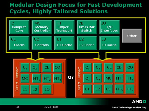
This type of approach makes a lot of sense in today's world. Designing processors without the need to reengineer the entire CPU from the ground up in order to add another compute core, HT link or (maybe) another memory controller is a stroke of brilliance. Dual and quad core systems don't need 2 or four of everything, but needs do change depending on the application targeted by the hardware. Hopefully AMD will use this technology to enable the delivery of changing CPU configurations much the same way we see clock speeds and cache sizes change over time today.
On a very slightly lower level architecture side, we have a slide showing the overview of AMD's next server class processor with 4 cores based on K8L. Features include a shared L3 cache, "enhanced IPC" cores, OoO (Out of Order) loads, wider data paths, HT-3 (the third version of HyperTransport), and support for DDR2 (and DDR3 or FBDIMMS in the future). Details on some of these enhancements were way too light, especially on the IPC (Instructions Per Clock) front.
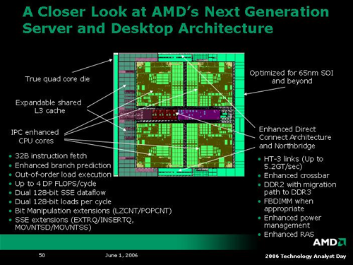
Cache enhancements include the capability to support 2x128-bit loads per cycle from the 64k L1 cache (which is half the size of the K8 L1 cache), and a shared L3 cache which will scale up from its introduction at 2MB. The shared L3 cache will help with features like node interleaving on multiprocessor systems as well as multithreaded apps which make use of shared data. We are still waiting for more detailed data on the cache architecture. It isn't clear whether the caches are all exclusive, and we would like to know more about associativity as well.
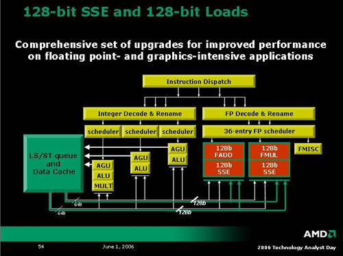
At a lower level, we have a block diagram of the compute core for K8L CPUs. Again, this diagram is a bit oversimplified, but we can see a few key features of the architecture. On the FP side, the CPU is able to handle 2x128-bit floating point or SSE operations per clock. While this isn't quite as flexible as Intel's Core with its 3 SSE units, AMD's K8L will be able to handle 4 double precision floating point operations per clock. . (Current K8 chips can only do 1x128/2x64-bit SSE instructions per clock.)
As with K8, K8L will have 3 ALUs (arithmetic logic units) and 3 AGUs (address generation units). Combined with cache enhancements and the new ability to reorder loads, K8L has a shot at outpacing Core in integer performance. Of course, we do still need more detail in this area to understand fully what's going on. No doubt, if AMD is claiming the ability to reorder loads, they can absolutely move loads ahead of loads (as this is the easiest case to handle). Where things get interesting is in the ability to move loads ahead of stores. Intel's Core architecture features some very interesting prediction technology in determining whether or not to move a load before a store. We haven't received an answer from AMD on whether they will tackle moving loads ahead of stores at all, let alone how they will handle memory disambiguation and/or prediction. In the past, we've seen a kind of "simpler is better" approach from AMD, so it will be interesting to see which direction K8L has taken.
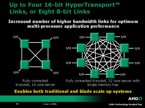
When it comes to processor interconnect technology, AMD has led Intel since the introduction of the Opteron. With K8L comes a very interesting enhancement to the interconnect architecture: each of the four 16-bit HyperTransport links can be split into two 8-bit HyperTransport links. Apparently, each of the resulting eight 8-bit HT links will be coherent and will allow a direct connection to another processor. In large systems, this means direct access from one core to seven others plus I/O, resulting in the possibility of fully connected 8-way systems. In a quad core world, that would be 32 cores on one platform. AMD also indicates that these HT connections can be used to easily scale blade implementations as well.
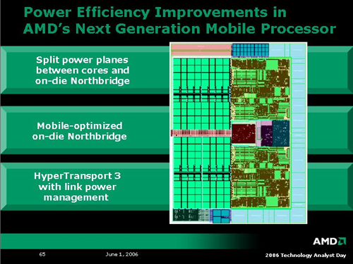
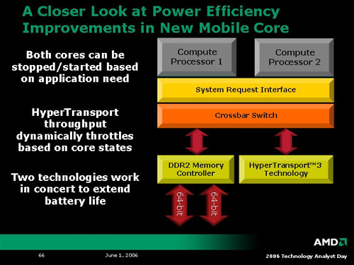
AMD mobile processors will also benefit from enhancements to HyperTransport with link power management. Not only will the new dual core 65nm K8L Turion processors be able to throttle cores independently, but even the HT links can be powered down when not in use. These enhancements will go a long way towards expanding AMD's mobile capabilities, especially if the K8L architecture can deliver better performance per Watt than the K8 before it. Compared to NetBurst architectures, K8 may as well have been an icebox, but that all changed with the introduction of Banias, Dothan, Yonah and now Core technology. Intel is bringing the fight to AMD, and K8L will need to deliver on the power front in order to remain competitive. The only market segment that really throws power to the wind is the extreme enthusiast (to which AMD's 4x4 initiative will certainly cater), but volume business will require an eye to the efficient.
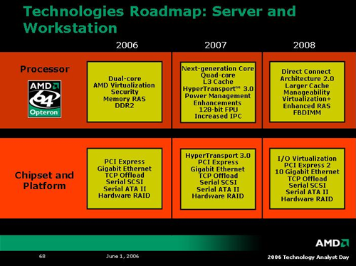
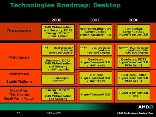
To round out what we learned about K8L architecture, here are the roadmap slides of technology AMD plans to roll out over the next three years.
At the outset, we hoped we'd have a very large section on AMD's new architecture. After our whirlwind of a three hour briefing, we aren't that much further along on the K8L architecture front than we were before. We've had some things confirmed by a few slides, but AMD didn't spend much time on these details. Over the next few days we will be sitting down with AMD and gathering as much detailed information about K8L as we can, but for now we can offer an overview of what we already know and have gathered from the slides we've seen.
The first K8L chips will be fabbed on a 65nm SOI process jointly developed by IBM and AMD, and manufactured at AMD facilities in Dresden. AMD has implemented a more modular approach to designing their next gen CPUs this time around in order to more easily meet the demands of a market craving ever increasing support for multicore technology. While CPUs are traditionally very hand tuned and designed on a low level, it appears AMD has taken an extremely object oriented approach to CPU design. The interfaces between different parts of the CPU are very strongly defined and it is possible for AMD to mix and match components as necessary.

This type of approach makes a lot of sense in today's world. Designing processors without the need to reengineer the entire CPU from the ground up in order to add another compute core, HT link or (maybe) another memory controller is a stroke of brilliance. Dual and quad core systems don't need 2 or four of everything, but needs do change depending on the application targeted by the hardware. Hopefully AMD will use this technology to enable the delivery of changing CPU configurations much the same way we see clock speeds and cache sizes change over time today.
On a very slightly lower level architecture side, we have a slide showing the overview of AMD's next server class processor with 4 cores based on K8L. Features include a shared L3 cache, "enhanced IPC" cores, OoO (Out of Order) loads, wider data paths, HT-3 (the third version of HyperTransport), and support for DDR2 (and DDR3 or FBDIMMS in the future). Details on some of these enhancements were way too light, especially on the IPC (Instructions Per Clock) front.

Cache enhancements include the capability to support 2x128-bit loads per cycle from the 64k L1 cache (which is half the size of the K8 L1 cache), and a shared L3 cache which will scale up from its introduction at 2MB. The shared L3 cache will help with features like node interleaving on multiprocessor systems as well as multithreaded apps which make use of shared data. We are still waiting for more detailed data on the cache architecture. It isn't clear whether the caches are all exclusive, and we would like to know more about associativity as well.
At a lower level, we have a block diagram of the compute core for K8L CPUs. Again, this diagram is a bit oversimplified, but we can see a few key features of the architecture. On the FP side, the CPU is able to handle 2x128-bit floating point or SSE operations per clock. While this isn't quite as flexible as Intel's Core with its 3 SSE units, AMD's K8L will be able to handle 4 double precision floating point operations per clock. . (Current K8 chips can only do 1x128/2x64-bit SSE instructions per clock.)
As with K8, K8L will have 3 ALUs (arithmetic logic units) and 3 AGUs (address generation units). Combined with cache enhancements and the new ability to reorder loads, K8L has a shot at outpacing Core in integer performance. Of course, we do still need more detail in this area to understand fully what's going on. No doubt, if AMD is claiming the ability to reorder loads, they can absolutely move loads ahead of loads (as this is the easiest case to handle). Where things get interesting is in the ability to move loads ahead of stores. Intel's Core architecture features some very interesting prediction technology in determining whether or not to move a load before a store. We haven't received an answer from AMD on whether they will tackle moving loads ahead of stores at all, let alone how they will handle memory disambiguation and/or prediction. In the past, we've seen a kind of "simpler is better" approach from AMD, so it will be interesting to see which direction K8L has taken.

When it comes to processor interconnect technology, AMD has led Intel since the introduction of the Opteron. With K8L comes a very interesting enhancement to the interconnect architecture: each of the four 16-bit HyperTransport links can be split into two 8-bit HyperTransport links. Apparently, each of the resulting eight 8-bit HT links will be coherent and will allow a direct connection to another processor. In large systems, this means direct access from one core to seven others plus I/O, resulting in the possibility of fully connected 8-way systems. In a quad core world, that would be 32 cores on one platform. AMD also indicates that these HT connections can be used to easily scale blade implementations as well.

AMD mobile processors will also benefit from enhancements to HyperTransport with link power management. Not only will the new dual core 65nm K8L Turion processors be able to throttle cores independently, but even the HT links can be powered down when not in use. These enhancements will go a long way towards expanding AMD's mobile capabilities, especially if the K8L architecture can deliver better performance per Watt than the K8 before it. Compared to NetBurst architectures, K8 may as well have been an icebox, but that all changed with the introduction of Banias, Dothan, Yonah and now Core technology. Intel is bringing the fight to AMD, and K8L will need to deliver on the power front in order to remain competitive. The only market segment that really throws power to the wind is the extreme enthusiast (to which AMD's 4x4 initiative will certainly cater), but volume business will require an eye to the efficient.


To round out what we learned about K8L architecture, here are the roadmap slides of technology AMD plans to roll out over the next three years.


40 Comments
View All Comments
MrKaz - Monday, June 5, 2006 - link
Did you talk someone at AMD if they have some one interested (or going to do) some SQL accelerator, or CAD calculations accelerator, or even multimedia accelerator accelerator?It would be nice to boost the performance of SQL by 2X, or even media encoding from minutes to seconds...
DerekWilson - Tuesday, June 6, 2006 - link
they are certainly talking heavily about the possibility of hardware like that, but no hardware designers have commited to building anything yet.IntelUser2000 - Sunday, June 4, 2006 - link
No. Because Core Duo(Yonah) with inferior decoder configuration, inferior memory bandwidth(which won't matter a lot but will make slight difference) and platform, still manages to outperform the current K8's. The Pentium M, which is even worse than Core Duo(slightly) still manages to outperform the K8's in integer. Now put Core with integrated memory controller, and comparison will look like Core Duo against Athlon XP.
Core microarchitecture will exceed K8's in general integer architecture, and at least equal in K8L's ability. Integer superiority is still gonna be there, K8L will be faster than Core in FP and SSE performance because of low latency integrated memory controller with lots more real-world bandwidth(well that depends on how AMD implements SSE, Intel may still have an advantage if AMD puts a poor implementation like they did with Athlon XP's SSE, or at least it looked poor).
JarredWalton - Sunday, June 4, 2006 - link
If ~33% of all instructions are Loads, and K8 pretty much totally lacks the ability to reorder Loads, adding that feature could substantially boost performance. It definitely "has a shot" at beating Core, but it may also fall short. Anyone making blanket statements one way or the other - i.e. it *will* beat Core, or it *won't* come close - needs to take a step back and check what they really know and what they are just assuming.At present, AMD is saying K8L is going to have the ability to reorder Loads. They might only do minor reordering, or they might go so far as to have something similar to Conroe's memory disambiguation. Given that AMD hasn't done a major update to K8 in over 3 years (no, DDR2 controller and going dual core don't really count as major updates to the underlying architecture), K8L could be a lot of things. It migth only match Core Duo 2 on a clock-for-clock basis; it might fall short; it might even come out ahead. Also, there has been no indication that Intel is seriously planning on-die memory controller in the near future, probably to continue to protect their chipset market.
Personally, I really hope AMD manages to basically match CD2 performance, because runaway performance leads don't help the consumer. In the end, theoretical integer, PF, SSE, etc. performance isn't as important as real-world application performance. Right now, it's just too soon to declare a victor in the Core Duo 2 vs. K8L match-up. CD2 vs. K8 is already pretty much a done deal, though, and there's no indication that AMD will be able to come out on top in that rivalry. K8L is their "counterattack", and that's the architecture that needs to compete with CD2.
IntelUser2000 - Sunday, June 4, 2006 - link
It's easy to see the performance in integer against Core. Core has ability to reorder loads, but Core Duo is in same situation as K8, it doesn't really have the ability either. Other than that, on the basic block diagram, K8 is superior architecturally to Core Duo, yet Integer performance is somewhat better on Core Duo. The difference probably goes deeper than that. One of the articles mention K7/K8 has similar technique to Intel's micro op fusion. It could be Intel's is much better, etc. If a K8 with substantially better microarchitecture(+ODMC) can't beat integer performance of Core Duo, will K8L with basically same microarchitecture(or may be worse) beat Core?? It's simple to see it probably won't.
DerekWilson - Tuesday, June 6, 2006 - link
core duo can reorder loads as the Pentium M could reorder loads --http://anandtech.com/cpuchipsets/showdoc.aspx?i=27...">http://anandtech.com/cpuchipsets/showdoc.aspx?i=27...
MrKaz - Monday, June 5, 2006 - link
P3 on steroids may beat the K7 on steroids in performance.But performance isn’t everything or Intel employees where out of job since K7 came out and beat P3 and P4. And Intel didnt recover yet!
I didn’t see any presentation of Intel new architecture, but I bet even the Hammer look better than any thing Intel will release.
http://www.amd.com/us-en/assets/content_type/Downl...">http://www.amd.com/us-en/assets/content...ableAsse...
4MB cache, 128bit SSE that tells me nothing. Other than the P3 started with PC100 SDRAM, 256Kb cache and SSE and it's now at DDR2 667, 4MB cache and SSE4.
Sceptor - Saturday, June 3, 2006 - link
Finally a real interconnect that can be used for a serious co-processor...perhaps a physics co-pro not limited by the PCI bus would help smooth transition to more realistic games.Or a dedicated video co-pro to use with Cad or 3D Modeling programs...
od4hs - Friday, June 2, 2006 - link
http://images.anandtech.com/reviews/cpu/amd/analys...">http://images.anandtech.com/reviews/cpu/amd/analys...
-> UK firm to unveil wall-socket PC
The Jack PC thin client fits into a wall socket and is so energy-efficient it can get its power over Ethernet
http://news.zdnet.co.uk/0,39020330,39272166,00.htm">http://news.zdnet.co.uk/0,39020330,39272166,00.htm
lopri - Friday, June 2, 2006 - link
I totally agree that the "direct connect" is the most desirable way but I cannot help but think AMD is somewhat daydreaming. That is, what's showing in the slides seems way ahead of today's "practicality".I mean, we've had this PCI Express which has been strongly pushed by core logic vendors, but so far all we practically have are video cards. I sometimes think all these mobo makers pay more attention to "asthetic" point when they design PCI-E slots so the boards look prettier. (lol)
If my understanding is correct, AMD will introduce a new type of slot, HTX, on motherboards. Will other technology/market follow? Or will it just give another chance to graphics card manufacturers to push us to buy new cards? On today's desktop boards, basically everything is "integrated", sans video. I know that a video card has its own core and frame buffer, and transfers data via Hyper Transport, but if a physics card can utilize the HTX, what stops a video card from connecting directly to CPU, without passing the core logic or system memory?
I think this will also be closely related to the available bandwidth of HTX per CPU core (or cores), and I can't really think of any add-in board that'll prioritize the bandwidth other than video cards, (OK and the physics cards) even though the HTX will be an open standard. (look at the lazy/lame Creative)
A very desirable case would be where storage (hard disks) can take advantage of this "direct" connection but then again there is a such thing called "memory", so my imagination stops there. (maybe solid-state/I-Ram type of storage can make use of the HTX? Then what's the use of memory? Taking care of I/O?) Talking about I/O, I just thought it'd be interesting to see keyboards/mice connect to CPU via HTX. (Sorry I couldn't resist)
All in all, like the article says, this roadmap seems just too broad/ambiguous/futuristic. I'm not a CPU engineer so my thinking could be totaly off, though. If so, please enlighten.
lop